Reconstructed by Charles Sinnett 6/11/93
Email: cas@mentor.cc.purdue.edu
HTMLified by B. Watson 9/14/2001
Email: atari@hardcoders.org
(Editor's notes --BW)
(The TV picture according to Atari)
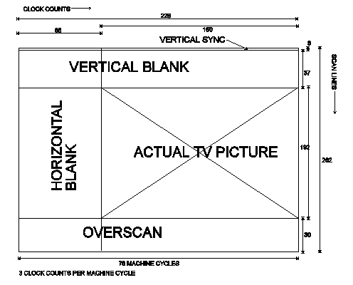
For the purposes of Stella programming, a single television "frame" consists of 262 horizontal lines, and each line is divided by 228 clock counts (3.58MHz). The actual TV picture is drawn line by line from the top down 60 times a second, and actaully consists of only a portion of the entire "frame" (see diag. #1). A typical frame will consists of 3 vertical sync (VSYNC) lines*, 37 vertical blank (VBLANK) lines, 192 TV picture lines, and 30 overscan lines. Atari's research has shown that this pattern will work on all types of TV sets. Each scan lines starts with 68 clock counts of horizontal blank (not seen on the TV screen) followed by 160 clock counts to fully scan one line of TV picture. When the electron beam reaches the end of a scan line, it returns to the left side of the screen, waits for the 68 horizontal blank clock counts, and proceeds to draw the next line below.All horizontal timing is taken care of by hardware, but the microprocessor must "manually" control vertical timing to signal the start of the next frame. When the last line of the previous frame is detected, the microprocessor must generate 3 lines of VSYNC, 37 lines of VBLANK, 192 lines of actual TV picture, and 30 lines of overscan. Fortunately, both VSYNC and VBLANK can simply be turned on and off at the appropriate times, freeing the microprocessor for other activities during their execution.
* (to signal the TV set to start a new frame)
The actual TV picture is drawn one line at a time by having the microprocessor enter the data for that line into the Television Interface Adaptor (TIA) chip, which then converts the data into video signals. The TIA can only have data in it that pertains to the line being currently drawn, so the microprocessor must be "one step ahead" of the electron beam on each line. Since one microprocessor machine cycle occurs every 3 clock counts, the programmer has only 76 machine cycles per line (228/3 = 76) to construct the actual picture (actually less because the microprocessor must be ahead of the raster). To allow more time for the software, it is customary (but not required) to update the TIA every two scan lines. The portion of the program that constructs this TV picture is referred to as the "Kernel", as it is the essence or kernel of the game.
In general, the remaining 70 scan lines (3 for VSYNC, 37 for VBLANK, and 30 for overscan) will provides 5,320 machine cycles (70 lines x 76 machine cycles) for housekeeping and game logic. Such activities as calculating the new position of a player, updating the score, and checking for new inputs are typically done during this time.
The TIA is a custom IC designed to create the TV picture and sound from the instructions sent to it by the microprocessor. It converts the 8 bit parallel data from the microprocessor into signals that are sent to video modulation circuits which combine and shape those signals to be compatible with ordinary TV reception. A "playfield" and 5 moveable objects can be created and manipulated by software.2.0 The RegistersA playfield consisting of walls, clouds, barriers, and other seldom moved objects can be created over a colored background. The 5 moveable objects can be positioned anywhere, and consists of 2 players, 2 missiles, and a ball. The playfield, players, missiles, and ball are created and manipulated by a series of registers in the TIA that the microprocessor can address and write into. Each type of object has certain defined capabilities. For example, a player can be moved with one instruction, but the playfield must be completely re-drawn in order to make it "move".
Color and luminosity (brightness) can be assigned to the background, playfield, and 5 moveable objects. Sound can also be generated and controlled for volume, pitch, and type of sound. Collisions between the various objects on the TV screen are detected by the TIA and can be read by the microprocessor . Input ports which can be read by the microprocessor give the status of some of the various hand held controllers.
All instructions to the TIA are achieved by addressing and writing to various registers in the chip. A key point to remember is data written in a register is latched an retained until altered by another write operation into that register. For example, if the color register for a player is set for red, that player will be red every time it is drawn until that color register is changed. All of the registers are addressed by the microprocessor as part of the overall RAM/ROM memory space.3.0 SynchronizationAll registers have fixed address locations and pre-assigned address names for handy reference. Many registers do not use all 8 data bits, and some registers are used to "strobe" or trigger events. A "strobe" register executes its function the instant it is written to (the data written is ignored). The only registers the microprocessor can read are the collision registers and input port registers. These registers are conveniently arranged so that the data bits of interest always appear as data bits 6 or 7 for easy access.
3.1 Horizontal Timing4.0 Color and LuminosityWhen the electron beam scans across the TV screen and reaches the right edge, it must be turned off and moved back to the left edge of the screen to begin the next scan line. The TIA takes care of this automatically, independent of the microprocessor. A 3.58 MHz oscillator generates clock pulses called "color clocks" which go into a pulse counter in the TIA. This counter allows 160 color clocks for the beam to reach the right edge, then generates a horizontal sync signal (HSYNC) to return the beam to the left edge. It also generates the signal to turn the beam off (horizontal blanking) during its return time of 68 color clocks. Total round trip for the electron beam is 160 + 68 = 228 color clocks. Again, all the horizontal timing is taken care of by the TIA without assistance from the microprocessor.3.2 Microprocessor Synchronization
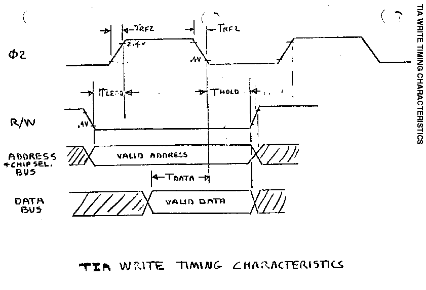
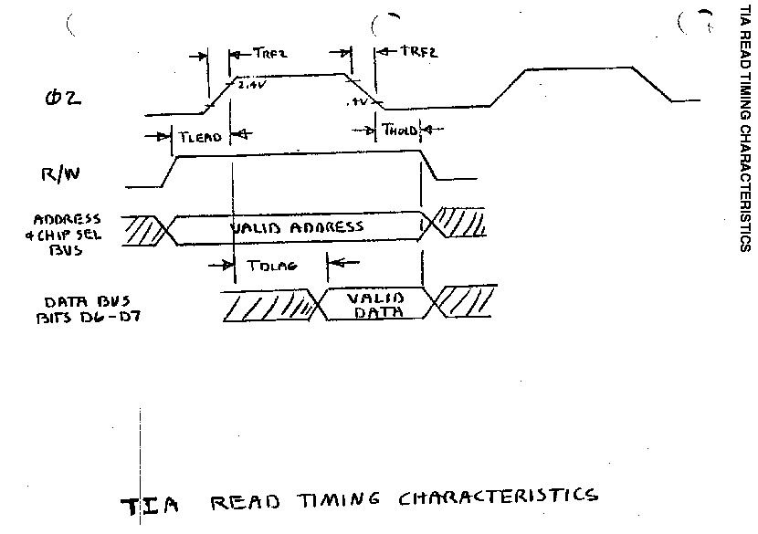
The microprocessor's clock is the 3.58 MHz oscillator divided by 3, so one machine cycle is 3 color clocks. Therefore, one complete scan line of 228 color clocks allows only 76 machine cycles (228/3 = 76) per scan line. The microprocessor must be synchronized with the TIA on a line-by-line basis, but program loops and branches take unpredictable lengths of time. To solve this software sync. problem, the programmer can use the WSYNC (Wait for SYNC) strobe register. Simply writing to the WSYNC causes the microprocessor to halt until the electron beam reaches the right edge of the screen, then the microprocessor resumes operation at the beginning of the 68 color clocks for horizontal blanking. Since the TIA latches all instructions until altered by another write operation, it could be updated every 2 or 3 lines. The advantage is the programmer gains more time to execute software, but at a price paid with lower vertical resolution in the graphics.3.3 Vertical timingNOTE: WSYNC and all the following addresses' bit structures are itemized in the TIA hardware manual. The purpose of this document is to make them understandable.
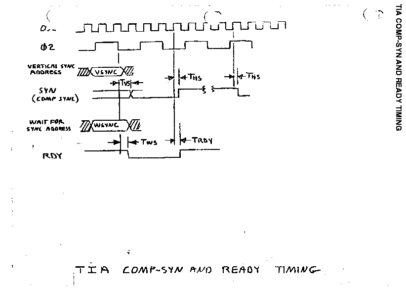
When the electron beam has scanned 262 lines, the TV set must be signaled to blank the beam and position it at the top of the screen to start a new frame. This signal is called vertical sync, and the TIA must transmit this signal for at least 3 scan lines. This is accomplished by writing a "1" in D1 of VSYNC to turn it on, count at least 2 scan lines, then write a "0" to D1 of VSYNC to turn it off.To physically turn the beam off during its repositioning time, the TV set needs 37 scan lines of vertical blanks signal from the TIA. This is accomplished by writing a "1" in D1 of VBLANK to turn it on, count 37 lines, then write a "0" to D1 of VBLANK to turn it off. The microprocessor is of course free to execute other software during the vertical timing commands, VSYNC and VBLANK.
Color and luminosity can be assigned to the background (BK), playfield (PF), ball (BL), player 0 (P0), player 1(P1), missile 0 (M0), and missile 1 (M1). There are only four color-lum registers for these 7 objects, so the objects are paired to share the same register according to the following list:5.0 Playfield
color-lum register Objects colored COLUMP0 P0, M0 (player 0, missile 0) COLUMP1 P1, M1 (player 1, missile 1) COLUMPF PF, BL (playfield, ball) COLUMBK BK (background) For example, if the COLUMP0 register is set for light red, both P0 and M0 will be light red when drawn.
A color-lum register is set for both color and luminosity by writing a single 7 bit instruction to that register. Four of the bits select one of the 16 available colors, and the other 3 bits select one of 8 levels of luminosity (brightness). The specific codes required to create specific color and lum are listed in the Detailed Address List of the TIA hardware manual. As with all registers (except the "strobe" registers), the data written to them is latched until altered by another write operation.
(These registers are referred to here as COLUMxx, but everywhere else they are COLUxx, including later in this document. --BW)
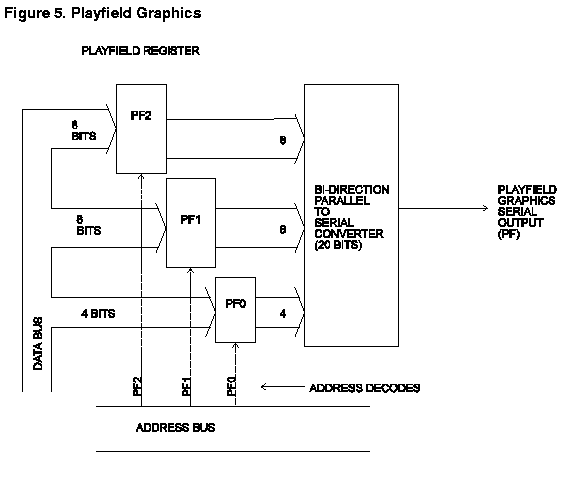
The PF register is used to create a playfield of walls, clouds, barriers, etc., that are seldom moved. This low resolution register is written into to draw the left half of the TV screen only. The right half of the screen is drawn by software selection of whether a duplication or a reflection of the right half.The PF register is 20 bits wide, so the 20 bits are written into 3 addresses: PF0, PF1, and PF2. PF0 is only 4 bits wide and constructs the first 4 "bits" of the playfield, starting at the left edge of the TV screen. PF1 constructs the next 8 "bits", and PF2 the last 8 bits" which end at the center of the screen. The PF register is scanned from left to right and where a "1" is found the PF color is drawn, and where a "0" is found, the BK color is drawn. To clear the playfield, obviously zeros must be written into PF0, PF1, and PF2.
To make the right half of the playfield into a duplication or copy of the left half, a "0" is written to D0 of the CTLPF (control playfield) register. Writing a "1" will cause the reflection to be displayed.
6.0 The Moveable Objects Graphics
6.1 Missile Graphics (M0, M1)All 5 moveable objects (P0, M0, P1, M1, BL) can be assigned a horizontal location on the screen and moved left or right relative to their location. Vertical positions, however, are treated in an entirely different manner. In principle, these objects appear at whatever scan lines their graphics registers are enabled. For example, let us assume the ball is to be positioned vertically in the center of the screen. The screen has 192 scan lines and we want the ball to be 2 scan lines "thick". The ball graphics would be disabled until scan line 96, enabled for 2 scan lines, then disabled for the rest of the frame. Each type of object (players, missiles, and ball) has its own characteristics and limitations.
The two missile graphics registers will draw a missile on any scan line by writing a "1" to the one bit enable missile registers (ENAM0, ENAM1). Writing a "0" to these registers will disable the graphics. The missiles' left edge is positioned by a horizontal position register, but the right edge is a function of how wide the missile is make. Width of a missile is controlled by writing into bits D4 and D5 of the number-size registers (NUSIZ0, NUSIZ1). This has the effect of "stretching" the missile out over 1,2,4, or 8 color clock counts (a full scan line is 160 color clocks).6.2 Ball Graphics (BL)
The ball graphics register works just like the missile registers. Writing a "1" to the enable ball register (ENABL) enables the ball graphics until the register is disabled. The ball can also be "stretched" to widths of 1, 2, 4, or 8 color clock counts by writing to bits D4 and D5 of the CTRLPF register.6.3 Player Graphics (P0, P1)The ball can also be vertically delayed one can line. For example, if the ball graphics were enabled on scan line 95, it could be delayed to not display on the screen until scan line 96 by writing a "1" to D0 of the vertical delay (VDELBL) register. The reason for having a vertical delay capability is because most programs will update the TIA every 2 lines. This confines all vertical movements of objects to 2 scan line "jumps". The use of vertical delay allows the objects to move one scan line at a time.
The player graphics are the most sophisticated of all the moveable objects. They have all the capabilities of the missile and ball graphics, plus three move capabilities. Players can take on a "shape" such as a man or an airplane, and the player can easily be flipped over horizontally to display the mirror image (reflection) instead of the original image, plus multiple copies of the players can be created.7.0 Horizontal PositioningThe player graphics are drawn line-by-line like all other graphics. The difference here is each scan line of the player is 8 "bits" wide, whereas the missiles and ball are one "bit" wide. Therefore, a player can be though of as being drawn of graph paper 8 squares wide and as tall as desired. To "color in the squares" of this imaginary graph paper, 8 data bits are written into the players graphics registers (GP0, GP1). This 8 bit register is scanned from D7 to D0, and wherever a "1" is found that "square" gets the players' color (from the color-lum register) and where a "0" is found that "square" gets the background color. To position a player vertically, simply leave all "0's" in the graphics registers (GP0, GP1) until the electron beam is on the scan line desired, write to the graphics register line-by-line describing the player, then write all "0's" to turn off the players' graphics until the end of that frame.
To display a mirror image (reflection) instead of the original figure, write a "1" to D3 of the one bit reflection register (REFP0, REFP1). A "0" written to these registers restores the original figure.
Multiple copies of players as well as their size are controlled by writing 3 bits (D0, D1, D2) into the number-size registers (NUSIZ0, NUSIZ1). These three bits select from 1 to 3 copies of the player, spacing of those copies, as well as the size of the player (each "square" of the player can be 1, 2, or 4 clocks wide). Whenever multiple copies are selected, the TIA automatically creates the same number of copies of the missile for that player. Again, the specifics of all this are laid out in the TIA hardware manual.
Vertical delay for the players works exactly like the ball by writing a "1" to D0 in the players' vertical delay registers (VDELP0, VDELP1). Writing a "0" to these locations disables the vertical delay.
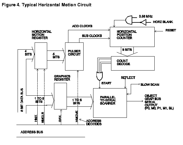
8.0 Horizontal MotionThe horizontal position of each object is set by writing to its associated reset register (RESP0, RESP1, RESM0, RESM1, RESBL) which are all "strobe" registers (they trigger their function as soon as they are addressed). That causes the object to be positioned wherever the electron bean was in its sweep across the screen when the register was reset. for example, if the electron beam was 60 color clocks into a scan line when RESP0 was written to, player 0 would be positioned 60 color clocks "in" on the next scan line. Whether or not P0 is actually drawn on the screen is a function of the data in the GP0 register, but if it were drawn, it would show up at 60. Resets to these registers anywhere during horizontal blanking will position objects at the left edge of the screen (color clock 0). Since there are 3 color clocks per machine cycle, and it can take up to 5 machine cycles to write the register, the programmer is confined to positioning the objects at 15 color clock intervals across the screen. This "course" positioning is "fine tuned" by the Horizontal Motion, explained in section 8.0.
Missiles have an additional positioning command. Writing a "1" to D1 of the reset missile-to-player register (RESMP0, RESMP1) disables that missiles' graphics (turns it off) and repositions it horizontally to the center of its associated player. Until a "0" is written to the register, the missile's horizontal position is locked to the center of its player in preparation to be fired again.
9.0 Object PrioritiesHorizontal motion allows the programmer to move any of the 5 graphics objects relative to their current horizontal position. Each object has a 4 bit horizontal motion register (HMP0, HMP1, HMM0, HMM1, HMBL) that can be loaded with a value in the range of +7 to -8 (negative values are expressed in two's complement from). This motion is not executed until the HMOVE register is written to, at which time all motion registers move their respective objects. Objects can be moved repeatedly by simply executing HMOVE. Any object that is not to move must have a 0 in its motion register. With the horizontal positioning command confined to positioning objects at 15 color clock intervals, the motion registers fills in the gaps by moving objects +7 to -8 color clocks. Objects can not be placed at any color clock position across the screen. All 5 motion registers can be set to zero simultaneously by writing to the horizontal motion clear register (HMCLR).
There are timing constraints for the HMOVE command. The HMOVE command must immediately follow a WSYNC (Wait for SYNC) to insure the HMOVE operation occurs during horizontal blanking. This is to allow sufficient time for the motion registers to do their thing before the electron beam starts drawing the next scan line. Also, for mysterious internal hardware considerations, the motion registers should not be modified for at least 24 machine cycles after an HMOVE command.
10.0 CollisionsEach object is assigned a priority so when any two objects overlap the one with the highest priority will appear to move in front of the other. To simplify hardware logic, the missiles have the same priority as their associated player, and the ball has the same priority as the playfield. The background, of course, has the lowest priority. The following table illustrates the normal (default) priority assignments.
Priority Objects 1 P0, M0 2 P1, M1 3 BL, PF 4 BK This priority assignment means that players and missiles will move in front of the playfield. To make the players and missiles move behind the playfield, a "1" must be written to D2 of the CTRLPF register. The following table illustrates how the priorities are affected:
Priority Objects 1 BL, PF 2 P0, M0 3 P1, M1 4 BK One more priority control is available to be used for displaying the score. When a "1" is written to D1 of the CTRLPF register, the left half of the playfield takes on the color of player 0, and the right half the color of player 1. The game score can now be displayed using the PF graphics register, and the score will be in the same color as its associated player.
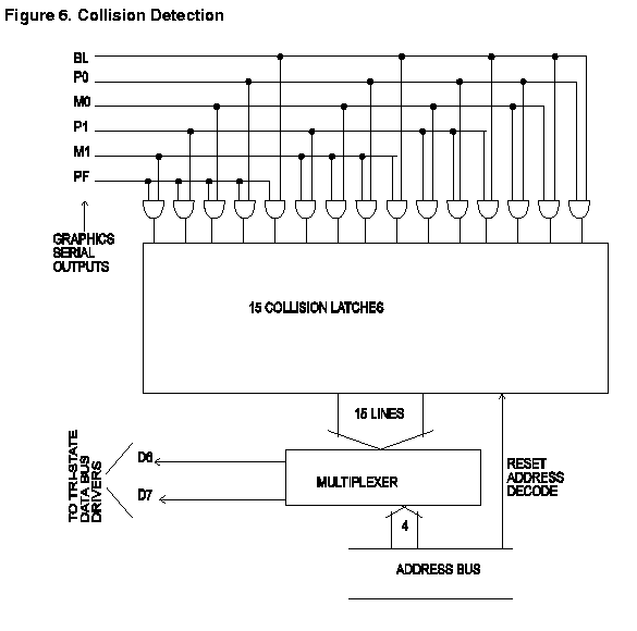
11.0 SoundThe TIA detects collisions between any of the 6 objects it generates (the playfield and 5 moveable objects). There are 15 possible two-object collisions which are stored in 15 one bit latches. Each collision register contains two of these latches which are read by the microprocessor on D6 and D7 of the data bus for easy access. A "1" on the data line indicates the collision it records has occurred. The collision registers could be read at any time but is usually done during vertical blank after all possible collisions have occurred. The collision registers are all reset simultaneously by writing to the collision reset register (CXCLR).
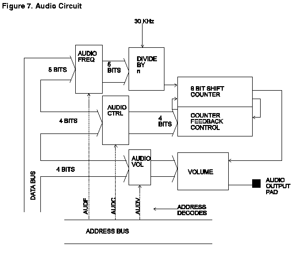
12.0 Input PortsThere are two audio circuits for generating sound. They are identical but completely independent and can be operated simultaneously to produce sound effects through the TV speaker. Each audio circuit has three registers that control a noise-tone generator (what kind of sound), a frequency selection (high or low pitch of the sound), and a volume control.
The noise-tone generator is controlled by writing to the 4 bit audio control registers (AUDC0, AUDC1). The values written cause different kinds of sounds to be generated. Some are pure tones like a flute, others have various "noise" content like a rocket motor or explosion. Even though the TIA hardware manual lists the sounds created by each value, some experimentation will be necessary to find "your sound".11.2 Frequency
Frequency selection is controlled by writing to a 5 bit audio frequency register (AUDF0, AUDF1). The value written is used to divide a 30KHz reference frequency creating higher or lower pitch of whatever type of sound is created by the noise-tone generator. By combining the pure tones available from the noise-tone generator with frequency selection a wide range of tones can be generated.11.3 Volume
Volume is controlled by writing to a 4 bit audio volume register (AUDV0, AUDV1). Writing 0 to these registers turns sound off completely, and writing any value up to 15 increases the volume accordingly.
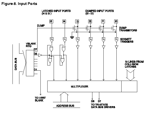
There are six input ports whose logic states can be read on D7 by reading the input port addresses (INPT0, thru INPT5). These six ports are divided into two types, "dumped" and "latched".
12.1 Dumped Input Ports (INPT0 thru INPT3)
These four ports are used to read up to four paddle controllers. Each paddle controller contains an adjustable pot controlled by the knob on the controller. The output of the pot is used to charge a capacitor in the console, and when the capacitor is charged the input port goes HI. The microprocessor discharges this capacitor by writing a "1" to D7 of VBLANK then measures the time it takes to detect a logic one at that port. This information can be used to position objects on the screen based on the position of the knob on the paddle controller.12.2 Latched Input Ports (INPT4, INPT5)
These two ports have latches that are both enabled by writing a "1" or disabled by writing a "0" to D6 of VBLANK. When disabled the microprocessor reads the logic level of the port directly. When enabled, the latch is set for logic one and remains that way until its port goes LO. When the port goes LO the latch goes LO and remains that way regardless of what the port does. The trigger buttons of the joystick controllers connect to these ports.
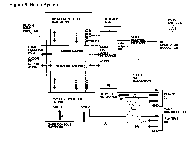
The PIA chip is an off-the-shelf 6532 Peripheral Interface Adaptor which has three functions: a programmable timer, 128 bytes of RAM, and two 8 bit parallel I/O ports.2.0 Interval timer
The PIA uses the same clock as the microprocessor so that one PIA cycle occurs for each machine cycle. The PIA can be set for one of four different "intervals", where each interval is some multiple of the clock (and therefore machine cycles). A value from 1 to 255 is loaded into the PIA which will be decremented by one at each interval. The timer can now be read by the microprocessor to determine elapsed time for timing various software operations and keep them synchronized with the hardware (TIA chip).
The timer is set by writing a value or count (from 1 to 255) to the address of the desired interval setting according to the following table :2.2 Reading the timer
Hex Address Interval Mnemonic 294 1 clock TIM1T 295 8 clocks TIM8T 296 64 clocks TIM64T 297 1024 clocks T1024T For example, if the value of 100 were written to TIM64T (HEX address 296) the timer would decrement to 0 in 6400 clocks (64 clocks per interval x 100 intervals) which would also be 6400 microprocessor machine cycles.
The timer may be read any number of times after it is loaded of course, but the programmer is usually interested in whether or not the timer has reached 0. The timer is read by reading INTIM at hex address 284.2.3 When the timer reaches zero
The PIA decrements the value or count loaded into it once each interval until it reaches 0. It holds that 0 counts for one interval, then the counter flips to FF(HEX) and decrements once each clock cycle, rather than once per interval. The purpose of this feature is to allow the programmer to determine how long ago the timer zeroed out in the event the timer was read after it passed zero.
The PIA has 128 bytes of RAM located in the Stella memory map from HEX address 80 to FF. The microprocessor stack is normally located from FF on down, and variables are normally located from 80 on up (hoping the two never meet).4.0 The I/O ports
5.0 Port A - Hand ControllersThe two ports (Port A and Port B) are 8 bits wide and can be set for either input or output. Port A is used to interface to carious hand-held controllers but Port B is dedicated to reading the status of the Stella console switches.
4.1 Port B - Console Switches (read only)
Port B is hardwired to be an input port only that is read by addressing SWCHB (HEX 282) to determine the status of all the console switches according to the following table:
Data Bit Switch Bit Meaning D7 P1 difficulty 0 = amateur (B), 1 = pro (A) D6 P0 difficulty 0 = amateur (B), 1 = pro (A) D5/D4 (not used) D3 color - B/W 0 = B/W, 1 = color D2 (not used) D1 game select 0 = switch pressed D0 game reset 0 = switch pressed
Port A is under full software control to be configured as an input or an output port. It can then be used to read or control various hand-head controllers with the data bits defined differently depending on the type of controller used.
5.1 Setting for input or output
Port A has an 8 bit wide Data Direction Register (DDR) that is written to at SWACNT (HEX 281) to set each individual pin of Port A to either input or output. The Port A pins are labeled PA0 thru PA7, and writing a "0" to a pins' DDR bit sets that pin as input, and a "1" sets it as an output. For example, writing all 0's to SWACNT (the DDR for Port A) sets PA0 thru PA7 (all 8 pins of Port A) as inputs. If F0 (11110000) were written to SWACNT then PA7, PA6, PA5 & PA4 would be outputs, and PA3, PA2, PA1 & PA0 would be inputs.Once the DDR has set the pins of Port A for input or output they may be read or written to by addressing SWCHA (HEX 280).Two joysticks can be read by configuring the entire port as input and reading the data at SWCHA according to the following table:5.4 Paddle (pot) controllers
A "0" in a data bit indicates the joystick has been moved to close that switch. All "1's" in a player's nibble indicates that joystick is not moving.(P0 = left player, P1 = right player)
Data Bit Direction Player D7 right P0 D6 left P0 D5 down P0 D4 up P0 D3 right P1 D2 left P1 D1 down P1 D0 up P1
Only the paddle triggers are read from the PIA. The paddles themselves are read at INP0 thru INPT3 of the TIA. The paddle triggers can be read at SWCHA according to the following table :5.5 Keyboard controllers
Data Bit Paddle # D7 P0 D6 P1 D5/D4 (not used) D3 P2 D2 P3 D1/D0 (not used)
The keyboard controller has 12 buttons arranged into 4 rows and 3 columns. A signal is sent to a row, then the columns are checked to see if a button is pushed, then the next row is signaled and all columns sensed, etc. until the entire keyboard is scanned and sensed. The PIA sends the signals to the rows, and the columns are sensed by reading INPT0, INPT1, and INPT4 of the TIA. With Port A configured as an output port, the data bits will send a signal to the keyboard controller rows according to the following table :
(P0 = left player, P1 = right player)
Data Bit Keyboard Row Player D7 bottom P0 D6 third P0 D5 second P0 D4 top P0 D3 bottom P1 D2 third P1 D1 second P1 D0 top P1 NOTE : a delay of 400 microseconds is necessary between writing to this port and reading the TIA input ports.
Hex Address Mnemonic Purpose 280 SWCHA Port A; input or output (read or write) 281 SWACNT Port A DDR, 0= input, 1=output 282 SWCHB Port B; console switches (read only) 283 SWBCNT Port B DDR (hardwired as input) 284 INTIM Timer output (read only) 294 TIM1T set 1 clock interval (838 nsec/interval) 295 TIM8T set 8 clock interval (6.7 usec/interval) 296 TIM64T set 64 clock interval (53.6 usec/interval) 297 T1024T set 1024 clock interval (858.2 usec/interval) NOTE: one clock is also one microprocessor machine cycle
PAL
1. The number of scan lines, and therefore the frame time increases from NTSC to PAL according to the following table:SECAM
NTSC PAL scanlines microseconds scanlines microseconds VBLANK 40 2548 48 3085 KERNEL 192 12228 228 14656 OVERSCAN 30 1910 36 2314 FRAME 262 16686 312 20055 2. Sounds will drop a little in pitch (frequency) because of a slower crystal clock. Some sounds may need the AUDF0/AUDF1 touched up.
3. PAL operates at 50 Hz compared to NTSC 60Hz, a 17% reduction. If game play speed is based on frames per second, it will slow down by 17%. This can be disastrous for most skill/action carts. If the NTSC version is designed with 2 byte fractional addition techniques (or anything not based on frames per second) to move objects, then PAL conversion can be as simple as changing the fraction tables, avoiding major surgery on the program.
1. SECAM is a little weird. It takes the PAL software, but the console color/black & white switch is hardwired as black & white. Therefore, it reads the PAL black & white tables in software and assigns a fixed color to each lum of black & white according to the following table:
Lum Color 0 Black 2 Blue 4 Red 6 Magenta 8 green A cyan C yellow E white There is a trap here: the manual is the same for NTSC, PAL, & SECAM. This means that the descriptions for black & white must jive between NTSC & PAL. If you make major changes to PAL black & white to achieve good SECAM color, NTSC black & white must be made similar.
2. PAL sounds work fine on SECAM with one exception: when a sound is to be turned off, it must be done by setting AUDV0/AUDV1 to 0, not by setting AUDC0/AUDC1 to 0. Otherwise, you get an obnoxious background sound.
The TIA is an MOS integrated circuit designed to interface between an eight (8) bit microprocessor and a television video modulator and to convert eight (8) bit parallel data into serial outputs for the color, luminosity, and composite sync required by a video modulator.DETAILED DESCRIPTIONThis circuit operates on a line by line basis, always outputting the same information every television line unless new data is written into it by the microprocessor.
A hardware sync counter produces horizontal sync timing independent of the microprocessor. Vertical sync timing is supplied to this circuit by the microprocessor and combined into composite sync.
Horizontal position counters are used to trigger the serial output of five (5) horizontally movable objects; two players, two missiles and a ball. The microprocessor can add or subtract from these position counters to move these objects right or left.
The microprocessor determines all vertical position and motion by writing zeros or ones into object registers before each appropriate horizontal line.
Walls, clouds and other seldom moved objects are produced by a low resolution data register called the playfield register.
A fifteen (15) bit collision register detects all fifteen possible two object collisions between these six (6) objects (five moveable and one playfield). This collision register can be read and reset by the microprocessor. Six input ports are also provided on this chip that can be read by the microprocessor. These input ports and the collision register are the only chip addresses that can be read by the microprocessor. All other addresses are write only.
Color luminosity registers are included that can be programmed by the microprocessor with eight (8) luminosity and fifteen (15) color values. A digital phase shifter is included on this chip to provide a single color output with fifteen (15) phase angles.
Two (2) independent audio generating circuits are included, each with programmable frequency, noise content, and volume control registers.
Registers on this chip are addressed by the microprocessor as part of its overall RAM-ROM memory space. The attached table of read-write addresses summarizes the addressable functions. There are no registers that are both read and write. Some addresses however are both read and write, with write data going into one register and read data returning from a different register.2. SynchronizationIf the read-write line is low, the data bits indicated in this table will be written into the addressed write location when the 02 clock goes from high to low. Some registers are eight bits wide, some only one bit, and some (strobes) have no bits, performing only control functions (such as resets) when their address is written.
If the read-write line is high, the addressed location can be read by the microprocessor on data lines 6 and 7 while the 02 clock is high.
The addresses given in the table refer only to the six (6) real address lines. If any of the four (4) chip select lines are used for addressing, the addresses must be modified accordingly.
3. Playfield graphics RegisterA. Horizontal Timing
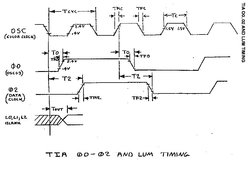
A hardware counter on this chip produces all horizontal timing (such as sync, blank, burst) independent of the microprocessor, This counter is driven from an external 3.58 Mhz oscillator and has a total count of 228. Blank is decoded as 68 counts and sync and color burst as 16 counts.B. Vertical Timing
There are one bit, addressable registers on this chip for vertical sync and vertical blank. The timing for these functions is established by the microprocessor by writing zero or one into these bits. (VSYNC, VBLANK )C. Composite Sync
Horizontal sync and the output of the vertical sync bit are combined together to produce composite sync. This composite sync signal drives a chip output pad to an external composite video resistor network.D. Microprocessor Synchronization
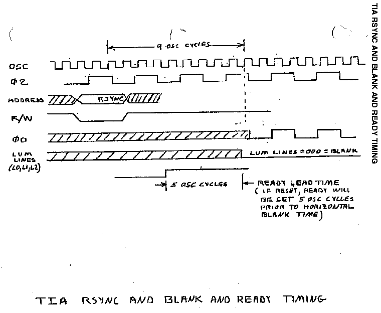
The 3.58 MHz oscillator also clocks a divide by three counter on this chip whose output (1.19 Mhz) is buffered to drive an output pad called 00. This pad provides the input phase zero clock to the microprocessor which then produces the system 02 clock (1.19 Mhz). Software program loops require different lengths of time to run depending on branch decisions made within the program. Additional synchronization between the software and hardware. This is done with a one bit latch called WSYNC (wait for sync). When the microprocessor finishes a routine such as loading registers for a horizontal line, or computing new vertical locations during vertical blank, it can address WSYNC, setting this latch high. When this latch is high, it drives an output pad to zero connected to the microprocessor ready line (RDY). A zero on this line causes the microprocessor to halt and wait. As shown in figure 2, WSYNC latch is automatically reset to zero by the leading edge of the next horizontal blank timing signal, releasing the RDY line, allowing the microprocessor to begin its computation and register writing for this horizontal television line or line pair.
A. Description4. Horizontal Position CountersObjects such as walls, clouds, and score) which are not required to move, are written into a 20 bit register called the playfield register. This register (Figure 5) is loaded from the data bus by three separate write addresses (PF0, PFl, PF2). Playfield may be loaded at any time. To clear the playfield, zeros must be written into all three addresses.B. Normal Serial Output
The playfield register is automatically scanned (and converted to serial output) by a bi-directional shift register clocked at a rate which spreads the twenty (20) bits out over the left half of a horizontal line. This scanning is initiated by the end of horizontal blank (left edge of television screen). Normally the same scan is then repeated, duplicating the same twenty (20) bit sequence over the right half of the horizontal line.C. Reflected Serial Output
A reflected playfield may be requested by writing a one into bit zero of the playfield control register (CTRLPF). When this bit is true the scanning shift register will scan the opposite direction during the right half of the horizontal line, reversing the twenty (20) bit sequence.D. Timing Constraints
Even though the playfield bytes (PF0, PFl, PF2) may be written to any time, if one of them is changed while being serially scanned, part of the new value may both show up on the television horizontal line.
5. Horizontal Motion RegistersA. Description
The playfield is a fixed graphics register, always starting its serial output when triggered by the beginning of each television line. This chip also includes five "moveable" graphics registers, whose serial outputs are triggered by five separate horizontal position counters every time these counters pass through zero count. These position counters are clocked continuously during the unblanked portion of every horizontal line and their count length is exactly equal to the normal number of clocks supplied to them during this time. They will therefore pass through zero at the same time during each horizontal television line and the triggered outputs will have no horizontal motion. A typical horizontal counter is shown in figure 4.B. Ball position CounterIf extra clocks are supplied to these counters (or normal clocks suppressed) the zero crossing time will shift and the object will have moved left (extra clocks) or right (fewer clocks). Some position counters have extra decoders (in addition to a zero decode) to trigger multiple copies of the same object across a horizontal line.
All position counters can be reset to zero count by the microprocessor at any time, by a write instruction to the reset addresses (RESBL, RESM0, RESMl, RESP0, RESPl). If reset occurs during horizontal blank, the object will appear at the left side of the television screen. Properly timed resets may position an object at any horizontal location consistent with the microprocessor cycle time.
The ball position counter has only the zero crossing decode and therefore cannot trigger multiple copies of the ball graphics.C. Player Position Counters
Each player position counter has three decodes in addition to the zero crossing decode. These decodes are controlled by bits 0,1,2 of the number size control registers (NUSIZ0, NUSIZ1), and trigger 1,2, or 3 copies of the player (at various spacings) across a horizontal line as shown on page ___. These same control bits are used for the decodes on the missile position counter, insuring an equal number of players and missiles.D. Missile Position CountersMissile position counters are identical to player position counters except that they have another type of reset in addition to the previously discussed horizontal position reset. These extra reset addresses (RESMP0, RESMP1) write data bit 1 into a one bit register whose output is used to position the missile (horizontally) directly on top of its corresponding player, and to disable the missile serial output.
A. General Description6. Moving Object Graphics RegistersThere are five write only registers on this chip that contain the horizontal motion values for each of the five moving objects. A typical horizontal motion register is shown in figure 4 . The data bus (bits 4 through 7) is written into these addresses (HMP0, HMPl, HMM0, HMMl, HMBL) to load these registers with motion values. These registers supply extra (or fewer) clocks to the horizontal position counters only when commanded to do so by an HMOVE address from the microprocessor. These registers may all be cleared to zero (no motion) simultaneously by an HMCLR command from the microprocessor, or individually by loading zeros into each register. These registers are each four bits in length and may be loaded with positive (left motion), negative (right motion) or zero (no motion) values. Negative values are represented in twos complement format.B. Timing constraints
These registers may be loaded or cleared at almost any time. The motion values they contain will be used only when an HMOVE command is addressed, and then all five motion values will be used simultaneously into all five horizontal position counters once. The only timing constraint on this operation involves the HMOVE command. The HMOVE command must be located in the microprocessor program immediately after a wait for sync (WSYNC) command. This assures that the HMOVE operation begins at the leading edge of horizontal blank, and has the full blank time to supply extra or fewer clocks to the horizontal position counters. These registers should not be modified for at least 24 Computer cycles after the HMOVE command.
A. General Description7. Collision Detection LatchesThere are five graphics registers for moving objects on this chip. These graphics registers are loaded (written) in parallel by the microprocessor and like the playfield register are scanned and converted to serial output. Unlike the playfield register, which is always scanned beginning at the left side of each horizontal line, moving object graphics registers are scanned only when triggered by a start decode from their horizontal position counter. A typical graphics register is shown in figure 4 .B. Missile Graphics
The graphics registers for both missiles are identical and very simple. They each consist of a one bit register called missile enable (ENAM0, ENAM1). This graphics bit is scanned (outputted) only when triggered by its corresponding position counter. There are control bits (bits 4, 5, of NUSIZ0, NUSIZ1) that can stretch this single graphics bit out over widths of 1, 2, 4, or 8 clocks of horizontal line time. (A full line is 160 clocks).C. Player Graphics
The graphics registers for both players are identical and are rather complex. They each consist of eight bit parallel registers (GRP0, GRP1) and a bi- directional parallel to serial scan counter that converts the parallel data into serial output. A one bit control register (REFP0, REFP1) determines the direction (reflection) of the parallel to serial scan, outputing either D7 through D0, or D0 though D7. This allows reflection (horizontal flipping) of player serial graphics data without having to flip the microprocessor data.D. Vertical DelayThe clock into the scan counter can be controlled (three bits of NUSIZ0 and NUSIZ1) to slow the scan rate and stretch the eight bits of serial graphics out over widths of 8, 16, or 32 clocks of horizontal line time. These same control bits are used in the player-missile motion counters to control multiple copies, so only three player widths ( scan rates) are available.
Each of the player graphics registers actually consists of two 8 bit parallel registers. The first (GRP0, GRP1) is loaded (written) from the microprocessor 8 bit data bus. The second is automatically loaded from the output of the first. The reason for this is a complex subject called vertical delay. A large amount of microprocessor time is required to generate player, missile and playfield graphics (table look up, masking, comparisons, etc.) and load these into this chip's registers. For most game programs this time is just too large to fit into one horizontal line time. In fact for most games it will barely fit into two line times (127 microseconds). Therefore, individual graphics registers are loaded (written) every two lines, and used twice for serial output between loads. This type of programing will obviously limit the vertical height resolution of objects to multiples of two lines. It also will limit the resolution of vertical motion to two lines jumps. Nothing can be done about the vertical height resolution; however, vertical motion can be resolved to a single line by addition of a second graphics register that is automatically parallel loaded from the output of the first, one line time after the first was loaded from the data bus. This second graphics register output is therefore always delayed vertically by one line. A control bit called vertical delay (VDEL0, VDEL1) selects which of these two registers is to be used for serial output. If this control bit is set by the microprocessor between picture frames, the object will be moved down (delayed) by one line during the next frame. In most programming applications player 0 graphics and player 1 graphics are loaded (written) alternately, during the blank time just prior to each line as shown in (figure 1). Since GRP0 and GRP1 addresses from the microprocessor alternate, they are delayed by one line from each other. The GRP0 address decode can therefore be used to load the delayed graphics register for player 1, and GRP1 likewise to load the delayed graphics register for player 0. The two vertical delay bits (VDEL0, VDELl) then select delayed or undelayed registers for player 0 and player 1 as serial outputs.E. Ball Graphics
The ball graphics register is almost identical to the missile graphics register. It also consists of a single enable bit (ENABL) whose output is triggered by the ball position counter. It also has two control bits (bits 4, 5 of CTRLPF) that can stretch this single graphics bit out over widths of 1, 2, 4, or 8 clocks of horizontal line time. Unlike the missile graphics; however, the ball graphics register has capability for vertical delay similar to the player graphics. A second graphics (enable) bit is alternately loaded from the output of the first, one line after the first was loaded from the data bus. A ball vertical delay bit (VDELBL) selects which of these two graphics bits is used for the ball serial output. The first graphics bit (ENABL) should be loaded during the same horizontal blank time as player 0 (GRP0), because GRP1 is used to load the second enable bit from the output of the first on alternate lines.
A. DefinitionsThe serial outputs from all the graphics registers represent real time horizontal location of objects on the television screen. If any of these outputs occur at the same time, they will overlap (collide) on the screen. There are six objects generated on this chip (five moving and playfield) allowing fifteen possible two object collisions. These overlaps (collisions) are detected by fifteen "and" gates whenever they occur, and are stored in fifteen individual latch register bits, as shown in figure 6.B. Reading Collision
The microprocessor can read these fifteen collision bits on data lines 6 and 7 by addressing them two at a time. This could be done at any time but is usually done between frames (during vertical blank) after all possible collisions have serially occurred.C. Reset
All collision bits are reset simultaneously by the microprocessor using the reset address CXCLR. This is usually done near the end of vertical blank, after collisions have been tested.
A. General Description8.5 Priority EncoderThere are 6 input ports on this chip whose logic state may be read on data line 7 with read addresses INPT0 through INPT5. These 6 ports are divided into two types, "dumped" and "latched". See Figure 8.B. Dumped Input Ports (I0 through I3)
These 4 input ports are normally used to read paddle position from an external potentiometer-capacitor circuit. In order to discharge these capacitors each of these input ports has a large transistor, which may be turned on (grounding the input ports) by writing into bit 7 of the register VBLANK. When this control bit is cleared the potentiometers begin to recharge the capacitors and the microprocessor measures the time required to detect a logic 1 at each input port.C. Latched Input ports (I4, I5)As long as bit 7 of register VBLANK is zero, these four ports are general purpose high impedance input ports. When this bit is a 1 these ports are grounded.
These two input ports have latches which can be enabled or disabled by writing into bit 6 of register VBLANK.When disabled, these latches are removed from the circuit completely and these ports become two general purpose input ports, whose present logic state can be read directly by the microprocessor.
When enabled, these latches will store negative (zero logic level) signals appearing on these two input ports, and the input port addresses will read the latches instead of the input ports.
When first enabled these latches will remain positive as long as the input ports remain positive (logic one). A zero input port signal will clear a latch value to zero, where it will remain (even after the port returns positive) until disabled. Both latches may be simultaneously disabled by writing a zero into bit 6 of register VBLANK.
A. Purpose9. Color Luminance RegistersAs discussed in the section on collisions, simultaneous serial outputs from the graphics registers represent overlap on the television screen. In order to have color-luminosity values assigned to individual objects it is necessary to establish priorities between objects when overlapped. The priority encoder is shown in figure 3.B. Priority Assignment
The lack of any objects results in a color-lum value called the background. The background (BK) has lowest priority and only appears when no objects are outputing. In order to simplify the logic, each missile is given the same color-lum value and priority as its corresponding player (P0, M0) and the ball is given the same color-lum value and priority as the playfield (PF, BL).C. Priority ControlThe following table illustrates the normal priority assignment:
Highest Priority P0, M0 Second Highest P1, M1 Third Highest PF, BL Lowest Priority BK Objects with higher priority will appear to move in front of objects with lower priority. Players will therefore move in front of playfield (clouds, walls, etc.).
There are two playfield control bits that affect priority, one called playfield priority (PFP) (bit 2 of CTRLPF) and one called score (bit 1 of CTRLPF). When a one is written into the PFP bit the priority assignment is modified as shown below.
Highest Priority PF, BL Second Highest P0, M0 Third Highest P1, M1 Lowest Priority BK Players will then move behind playfield (clouds, wall, etc.). When a one is written into the score control bit, the playfield is forced to take the color-lum of player 0 in the left half of the screen and player 1 in the right half of the screen. This is used when displaying score and identifies the score with the correct player. The priority encoder produces 4 register select lines shown in figure 3) that are mutually exclusive. These 4 lines select either background, player 0, player 1 or playfield, and only one of them can be true at a time.
A. Description10. Color Phase ShifterThere are four registers (shown in figure 3) that contain color-lum codes. Four bits of color code and three its of luminance code may be written into each of these registers (COLUP0, COLUP1, COLUPF, COLUBK) by the microprocessor at any time. These codes (representing 16 color values and 8 luminance values) are given in the Detailed Address List.B. Multiplexing
The serial graphics output from all six objects is examined by the priority encoder which activates one of the four select lines into a 4 x 7 multiplexer. This multiplexer (shown in figure 3) then selects one of the four color-lum registers as a 7 line output. Three of these lines are binary coded luminosity and go directly to chip output pads. The other four lines go to the color phase shifter.
This portion of the chip (shown in figure 3) produces a reference color output (color burst) during horizontal blank and then during the unblanked portion of the line it produces a color output shifted in phase with respect to the color burst. The amount of phase shift determines the color and is selected by the four color code lines from the Color-lum multiplexer. Binary code 0 selects no color. Code 1 selects gold (same phase as color burst). Codes 2 (0010) through 15 (1111) shift the phase from zero through almost 360 degrees allowing selection of 15 total colors around the television color wheel.11. Audio Circuits
Two audio circuits are incorporated on this chip. They are identical and completely independent, although their outputs could be combined externally into one speaker. Each audio circuit consists of parts described below, and in figure 7.A. Frequency Select
Clock pulses (at approximately 30 KHz) from the horizontal sync counter pass through a divide by N circuit which is controlled by the output code from a five bit frequency register (AUDF). This register can be loaded (written) by the microprocessor at any time, and causes the 30 KHz clocks to be divided by 1 (code 00000) through 32 (code 11111). This produces pulses that are digitally adjustable from approximately 30 KHz to 1 KHz and are used to clock the noise-tone generator.B. Noise-Tone GeneratorThis circuit contains a nine bit shift counter which may be controlled by the output code from a four bit audio control register(AUDC), and is clocked by the frequency select circuit. The control register can be loaded by the microprocessor at any time, and selects different shift counter feedback taps and count lengths to produce a variety of noise and tone qualities.C. Volume Select
The shift counter output is used to drive the audio output pad through four driver transistors that are graduated in size. Each transistor is twice as large as the previous one and is enable by one bit from the audio volume register (AUDV). This audio volume register may be loaded by the microprocessor at any time. As binary codes 0 through 15 are loaded, the pad drive transistors are enabled in a binary sequence. The shift counter output therefore can pull down on the audio output pad with 16 selectable impedance levels.
Figure 2. Synchronization
Figure 3. Color-LuminanceFigure 4. Typical Horizontal Motion Circuit
Write Address Detailed Functions
This address halts microprocessor by clearing RDY latch to zero. RDY is set true again by the leading edge of horizontal blank.RSYNC (reset sync)Data bits not used
This address resets the horizontal sync counter to define the beginning of horizontal blank time, and is used in chip testing.VSYNCData bits not used.
This address controls vertical sync time by writing D1 into the VSYNC latchVBLANK
D1 0 Stop vertical sync 1 Start vertical sync This address controls vertical blank and the latches and dumping transistors on the input ports by writing into bits D7, D6 and D1 of the VBLANK register.PF0 (PF1, PF2)Note : Disable latches (D6 = 0) also resets latches to logic true
Data Bit Value Effect D1 0 Stop vert. blank 1 Start vert. blank D6 0 Disable INPT4, INPT5 latches 1 Enable INPT4, INPT5 latches D7 0 Remove INPT1,2,3,6 dump path to ground 1 Dump INPT1,2,3,6 to ground These addresses are used to write into playfield registersPLAYFIELD REGISTERS SERIAL OUTPUT
PF0 D7 D6 D5 D4 (not used) PF1 D7 D6 D5 D4 D3 D2 D1 D0 PF2 D7 D6 D5 D4 D3 D2 D1 D0 CTRLPF
1 horizontal line ( 160 clocks) Playfield Reflect Control 4..7 7......0 0......7 4..7 7......0 0......7 REF = 0 PF0 PF1 PF2 PF0 PF1 PF2 center
4..7 7......0 0......7 7......0 0......7 7..4 REF = 1 PF0 PF1 PF2 PF2 PF1 PF0 each bit = 4 clocks
This address is used to write into the playfield control register (a logic 1 causes action as described below)NUSIZ0 (NUSIZ1)
D0 REF (reflect playfield) D1 SCORE (left half of playfield gets color of player 0, right half gets color of player D2 PFP (playfield gets priority over players so they can move behind the playfield) D4 Ball Size (see next table) D5 D4 & D5 = BALL SIZE
D5 D4 Width 0 0 1 clock 0 1 2 clocks 1 0 4 clocks 1 1 8 clocks These addresses control the number and size of players and missiles.RESP0 (RESP1, RESM0, RESM1, RESBL)Missile Size
D5 D4 Width 0 0 1 clock 0 1 2 clocks 1 0 4 clocks 1 1 8 clocks Player-Missile number & player size
D2 D1 D0 1/2 television line (80 clocks)
8 clocks per squareDescription 0 0 0 X one copy 0 0 1 X X two copies - close 0 1 0 X X two copies - med 0 1 1 X X X three copies - close 1 0 0 X X two copies - wide 1 0 1 X X double size player 1 1 0 X X X 3 copies medium 1 1 1 X X X X quad sized player These addresses are used to reset players, missiles and the ball. The object will begin its serial graphics at the time of a horizontal line at which the reset address occurs.RESMP0 (RESMP1)No data bits are used
These addresses are used to reset the horiz. location of a missile to the center of its corresponding player. As long as this control bit is true (1) the missile will remain locked to the center of its player and the missile graphics will be disabled. When a zero is written into this location, the missile is enabled, and can be moved independently from the player.HMOVE
D1 = RESMP (missile-player reset)This address causes the horizontal motion register values to be acted upon during the horizontal blank time in which it occurs. It must occur at the beginning of horiz. blank in order to allow time for generation of extra clock pulses into the horizontal position counters if motion is desired this command must immediately follow a WSYNC command in the program.HMCLRNo data bits are used.
This address clears all horizontal motion registers to zero (no motion). No data bits are used.HMP0 (HMP1, HMM0, HMM1, HMBL)These addresses write data (horizontal motion values) into the horizontal motion registers. These registers will cause horizontal motion only when commanded to do so by the horiz. move command HMOVE. The motion values are coded as shown below :ENAM0 (ENAM1, ENABL)WARNING : These motion registers should not be modified during the 24 computer cycles immediately following an HMOVE command. Unpredictable motion values may result.
D7 D6 D5 D4 Clocks Effect 0 1 1 1 +7 Move left indicated number of clocks 0 1 1 0 +6 0 1 0 1 +5 0 1 0 0 +4 0 0 1 1 +3 0 0 1 0 +2 0 0 0 1 +1 0 0 0 0 0 No Motion 1 1 1 1 -1 Move right indicated number of clocks 1 1 1 0 -2 1 1 0 1 -3 1 1 0 0 -4 1 0 1 1 -5 1 0 1 0 -6 1 0 0 1 -7 1 0 0 0 -8 These addresses write D1 into the 1 bit missile or ball graphics registers.GRP0 (GRP1)
D1 0 Disables object 1 Enables object These addresses write data into the player graphics registers.REFP0 (REFP1)Note: serial output begins with D7, unless REFP0 (REFP1) = 1
D7 D6 D5 D4 D3 D2 D1 D0 Graphics Data These addesses write D3 into the 1 bit player reflect registersVDELP0 (VDELP1, VDELBL)
D3 0 no reflect, D7 of GRPx on left 1 reflect, D0 of GRPx on left These addresses write D0 into the 1 bit vertical delay registers, to delay players or ball by one vertical line.CXCLR
D0 0 no delay 1 delay This adderess clears all collision latches to zero (no collision). No data bits are used.COLUP0 (COLUP1, COLUPF, COLUBK)These addresses write data into the player, playfield, and background color-luminance registersAUDF0 (AUDF1)
COLOR D7 D6 D5 D4 D3 D2 D1 LUM grey - gold 0 0 0 0 0 0 0 black 0 0 0 1 0 0 1 dark grey orange, brt-org 0 0 1 0 0 1 0 0 0 1 1 0 1 1 grey pink - purple 0 1 0 0 1 0 0 0 1 0 1 1 0 1 purp-blue, blue 0 1 1 0 1 1 0 light grey 0 1 1 1 1 1 1 white blue - lt. blue 1 0 0 0 1 0 0 1 torq. - grn. blue 1 0 1 0 1 0 1 1 grn. - yel. grn. 1 1 0 0 1 1 0 1 org. grn - lt org. 1 1 1 0 1 1 1 1 These addresses write data into the audio frequency divider registers.AUDC0 (AUDC1)
D4 D3 D2 D1 D0 30KHz divided by 0 0 0 0 0 no division 0 0 0 0 1 divide by 2 0 0 0 1 0 divide by 3 ... ... ... ... ... ... 1 1 1 1 0 divide by 31 1 1 1 1 1 divide by 32 These addresses write data into the audio control registers which control the noise content and additional division of the audio output.AUDV0 (AUDV1)
D3 D2 D1 D0 Type of noise or division 0 0 0 0 set to 1 0 0 0 1 4 bit poly 0 0 1 0 div 15 -> 4 bit poly 0 0 1 1 5 bit poly -> 4 bit poly 0 1 0 0 div 2 : pure tone 0 1 0 1 div 2 : pure tone 0 1 1 0 div 31 : pure tone 0 1 1 1 5 bit poly -> div 2 1 0 0 0 9 bit poly (white noise) 1 0 0 1 5 bit poly 1 0 1 0 div 31 : pure tone 1 0 1 1 set last 4 bits to 1 1 1 0 0 div 6 : pure tone 1 1 0 1 div 6 : pure tone 1 1 1 0 div 93 : pure tone 1 1 1 1 5 bit poly div 6 These addresses write data into the audio volume registers which set the pull down impedance driving the audio output pads.
D3 D2 D1 D0 Audio Output Pull down current 0 0 0 0 No output current 0 0 0 1 lowest 0 0 1 0 ... ... ... ... 1 1 1 0 1 1 1 1 highest
TIA WRITE ADDRESS SUMMARY
6-bit Address Address Name 7 6 5 4 3 2 1 0 Function 00 VSYNC . . . . . . 1 . vertical sync set-clear 01 VBLANK 1 1 . . . . 1 . vertical blank set-clear 02 WSYNC strobe wait for leading edge of horizontal blank 03 RSYNC strobe reset horizontal sync counter 04 NUSIZ0 . . 1 1 1 1 1 1 number-size player-missile 0 05 NUSIZ1 . . 1 1 1 1 1 1 number-size player-missile 1 06 COLUP0 1 1 1 1 1 1 1 . color-lum player 0 07 COLUP1 1 1 1 1 1 1 1 . color-lum player 1 08 COLUPF 1 1 1 1 1 1 1 . color-lum playfield 09 COLUBK 1 1 1 1 1 1 1 . color-lum background 0A CTRLPF . . 1 1 . 1 1 1 control playfield ball size & collisions 0B REFP0 . . . . 1 . . . reflect player 0 0C REFP1 . . . . 1 . . . reflect player 1 0D PF0 1 1 1 1 . . . . playfield register byte 0 0E PF1 1 1 1 1 1 1 1 1 playfield register byte 1 0F PF2 1 1 1 1 1 1 1 1 playfield register byte 2 10 RESP0 strobe reset player 0 11 RESP1 strobe reset player 1 12 RESM0 strobe reset missile 0 13 RESM1 strobe reset missile 1 14 RESBL strobe reset ball 15 AUDC0 . . . . 1 1 1 1 audio control 0 16 AUDC1 . . . 1 1 1 1 1 audio control 1 17 AUDF0 . . . 1 1 1 1 1 audio frequency 0 18 AUDF1 . . . . 1 1 1 1 audio frequency 1 19 AUDV0 . . . . 1 1 1 1 audio volume 0 1A AUDV1 . . . . 1 1 1 1 audio volume 1 1B GRP0 1 1 1 1 1 1 1 1 graphics player 0 1C GRP1 1 1 1 1 1 1 1 1 graphics player 1 1D ENAM0 . . . . . . 1 . graphics (enable) missile 0 1E ENAM1 . . . . . . 1 . graphics (enable) missile 1 1F ENABL . . . . . . 1 . graphics (enable) ball 20 HMP0 1 1 1 1 . . . . horizontal motion player 0 21 HMP1 1 1 1 1 . . . . horizontal motion player 1 22 HMM0 1 1 1 1 . . . . horizontal motion missile 0 23 HMM1 1 1 1 1 . . . . horizontal motion missile 1 24 HMBL 1 1 1 1 . . . . horizontal motion ball 25 VDELP0 . . . . . . . 1 vertical delay player 0 26 VDELP1 . . . . . . . 1 vertical delay player 1 27 VDELBL . . . . . . . 1 vertical delay ball 28 RESMP0 . . . . . . 1 . reset missile 0 to player 0 29 RESMP1 . . . . . . 1 . reset missile 1 to player 1 2A HMOVE strobe apply horizontal motion 2B HMCLR strobe clear horizontal motion registers 2C CXCLR strobe clear collision latches
TIA READ ADDRESS SUMMARY
Note : I0, I2, I2, I3 can be grounded under software control. I4, I5 can be converted to latched inputs under software control
6-bit Address Address Name 7 6 5 4 3 2 1 0 Function D7 D6 0 CXM0P 1 1 . . . . . . read collision M0 P1 M0 P0 1 CXM1P 1 1 . . . . . . read collision M1 P0 M1 P1 2 CXP0FB 1 1 . . . . . . read collision P0 PF P0 BL 3 CXP1FB 1 1 . . . . . . read collision P1 PF P1 BL 4 CXM0FB 1 1 . . . . . . read collision M0 PF M0 BL 5 CXM1FB 1 1 . . . . . . read collision M1 PF M1 BL 6 CXBLPF 1 . . . . . . . read collision BL PF unused 7 CXPPMM 1 1 . . . . . . read collision P0 P1 M0 M1 8 INPT0 1 . . . . . . . read pot port 9 INPT1 1 . . . . . . . read pot port A INPT2 1 . . . . . . . read pot port B INPT3 1 . . . . . . . read pot port C INPT4 1 . . . . . . . read input D INPT5 1 . . . . . . . read input (For PIA I/O addresses, see section 6,0 --BW)
(This section is *not* part of the manual, so you can ignore it if you want! --BW)
I did this HTML version of the Stella Programming Guide for a couple of reasons:
- The existing PDF version is great, but I really hate having to use a PDF reader to read it. HTML is (supposedly) cross-platform, and since I already keep 10-15 browser windows open at any given time, I'd rather use the same GUI for reading the Stella docs as I do for everything else that's graphical.
- The existing plain-text version I found is ok, but it's missing all the diagrams (of course), and some of the text formatting is a bit strange.
- I tried numerous programs that claim to convert PDF (or PostScript) to HTML, but they all produced ugly, unusable results.
- I wanted internal links in the document, such as the table of contents. The existing PDF version doesn't seem to have them. The next version of this document will probably have links to external `how-to' docs, with code snippets and such.
- The Stella/Atari development community are some of the nicest people I've ever met, and this is my attempt to give back to the community in some small way.
- Finally, I needed an excuse to procrastinate... my poor 2600 game is in a nasty state of disrepair, and I'm at the point where I'd be better starting from scratch. Taking a break from 6502 asm and writing in a `language' like HTML gives me a much-needed breather.
The original PDF version has a few typos. I don't know if those are in the original paper version, or mistakes in the transcription, but I fixed as many of them as I could find (most of them were silly, like it's instead of its, or sidable for disable). Also, I didn't try to format the tables exactly as they appear in the PDF version, since HTML isn't much good for that sort of thing anyway. I did my best to preserve the content, but took a few liberties with the presentation.
Although I have tried to avoid it, I'm sure I introduced a few errors and typos of my own. If anybody spots one, let me know, and I'll fix it ASAP.
As far as copyright goes, who knows what the official, legal status of the Stella Programmer's Guide is? I sure don't. But this HTML version is free for anyone to use and/or redistribute, as much as the original version is. If you modify this version, I'd really appreciate it if you'd clearly mark your new version as modified. Better yet, if you fix some of my mistakes, show me what I did wrong so I can learn from them!
I looked at this in Netscape 4.7, Opera 5.0b6, and Konqueror 2.1 on Linux, and IE 5.0 on Win98; it looks OK on all of them. If you have any problems with the HTML formatting, please let me know. I tried to use `bog standard' HTML as much as possible, so it should work OK on any browser, on any OS, but if it doesn't, I'll fix it the best I am able.
B. Watson
atari@hardcoders.org
09/15/2001